Nano Dot Array

ND NANO DOT ARRAY

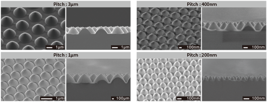
Nano dot array technology originated from Oji group enables fine fabrication ranging from hundreds nm to microns in pitch at the surface. Wide variety of applications has been presented for the customers such as optics, analytical chemistry, and life science/medical fields.

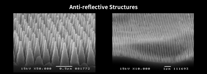
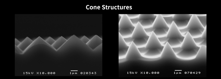
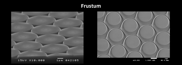
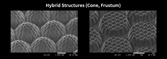
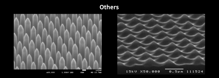
Various nano structures

Nano dot structures with various shape and size are fabricated. Customizations are available.

Electron microscope image of an antireflective structure. The structure is shown as a uniform array of microscopic sharp projections.
Electron microscope image of a conical structure. It shows a surface structure with conical protrusions arranged in a regular pattern.
Electron microscope image of a conical conical structure. It shows a microstructure of overlapping conical protrusions.
Electron microscope image of a composite structure. It shows the surface of a dense honeycomb of spherical structures.
Electron microscope images of other microstructures. Shown are regularly arranged microscopic protrusions and wavy surface patterns.

Various applications for wide technical fields


Application of Nano Dot Array 1, Specular anti-reflective structures (anti-reflection and improvement of transmittance for flat surface)

A film with moth-eye surface structure (Upper Fig. : nano sized dot-type structure) decreases reflectance (increases transmittance) of light.

Image showing the surface structure of an insect's eye and its magnified view. The microstructure is magnified on the right, and the reflectance graph shows that with structure (red line) the reflectance is 0.31% @555nm and without structure (yellow line) is 5.11% @555nm.
Comparative images of the outer surface of the plastic sheets. Reflected light can be seen on the left side without the mirror surface anti-reflection structure, but with the mirror surface anti-reflection structure on the right side, reflected light is suppressed and the image of the building is clearly displayed.

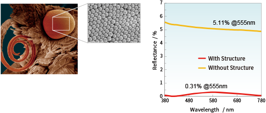
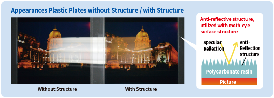
Films or plastic moldings with anti-reflective structure at the surface are available.

Application
Mirrored optical pats requiring low-reflectance and high-transmittance.
Materials
(Direct fabrication)Silicon, Quarts glass etc.
(Plastic molding)Acrylic resin, Poly styrene, Poly carbonate, Cycloolefin resin, etc.

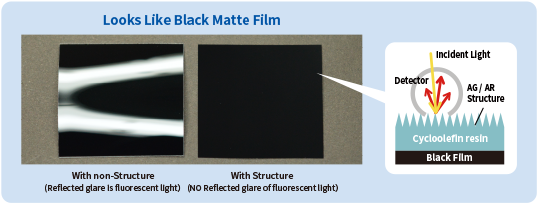
Application of Nano Dot Array 2, Anti-glare / Anti-reflective structures (anti-reflection of uneven surface)
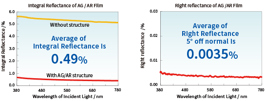
Absolutely black surface has been developed by Anti-glare / Anti-reflective structure, which enables reduction of reflection and glare from any incident angle*. Useful for reduction of stray light.

* Integral reflectance : < ca. 0.5%
Comparative images showing the effect of the diffuse anti-reflective structure film. On the left, the film without structure shows light reflection, and on the right, the film with structure shows a matte black surface with reduced light reflection. On the right, a diagram illustrating the mechanism of light diffusion and absorption by the microstructure is shown.
Two graphs showing reflectance data for diffuse anti-reflective structured films. The left graph shows the integral reflectance, with an average of 0.49% for the film with structure and a high reflectance for the film without structure. The graph on the right shows the positive reflectance, which averages 0.0035% for the structured film at an angle of incidence of 5°, indicating a low reflectance.
Application
Surface requiring low reflectance, e. g. inside of optical enclosure for reduction of stray light. (inside of camera and optical inspection instruments)
Materials
(Plastic molding)Acrylic resin, Poly styrene, Poly carbonate, Cyclo olefin resin, etc.

Application of Nano Dot Array 3, Sapphire Substrates with Fine Structure

Patterned sapphire substrate (PSS)* is available, which enables high light extraction efficiency. Fine fabrication is possible at the surface of the growth face of semiconductor crystal and the light extraction face of flip-chip type (opposite face of the growth face).

* PSS:Patterned Sapphire Substrate
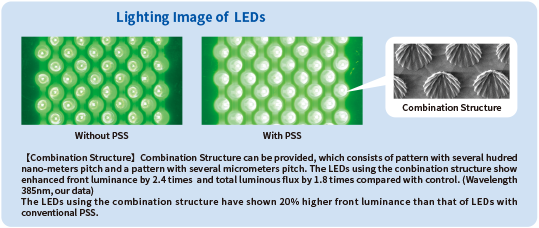
Comparison images of LEDs in lighting condition. On the left is an LED without PSS, with low light uniformity. On the right is an LED with PSS, with uniform light. The upper right shows an enlarged image of the composite structure, in which the fine pitch structure can be seen.
Electron microscope images of various microstructures that can be used for LEDs. The upper left shows a 3-μm pitch structure and the lower left shows a 1-μm pitch structure. The upper right shows a cross-sectional image of a 400 nm pitch structure, and the lower right shows a 200 nm pitch structure. Each structure forms a regularly arranged fine pattern.
Example of fine structures for LEDs
Application
Control of epitaxial growth on optical elements such as LEDs, Enhancement of light extraction efficiency by outcoupling effect, etc.
Materials
(Direct fabrication) Sapphire, Silicon carbide, Silicon, Quartz Glass, Gallium Nitride, etc.

Application of Nano Dot Array 4, Plasmonic Device

Device using surface plasmons

Fine structures are available which improve light extraction efficiency of OLEDs and enhance photoelectric conversion efficiency of Organic thin-film solar cells.
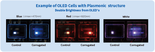
This image shows an example of surface plasmon structure introduced into an organic light emitting device. Comparison of a blue device (wavelength: 470 nm), a red device (wavelength: 620 nm), and a white device is shown. The light intensity is low without the microstructure, but the light intensity is increased with the microstructure, respectively.
Application
Improvement of brightness and reduction of power consumption of OLEDs, Enhancement of photo electric conversion efficiency of Organic thin-film solar cells, etc.
Materials
Quartz Glass, Ordinary glass, Silicon, Silicon Carbide, Sapphire, Plastic films, etc.

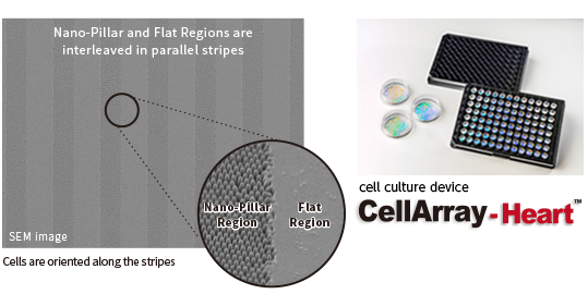
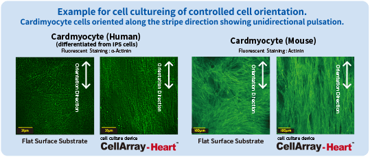
Application of Nano Dot Array 5, Cell culture substrates for controlled cell orientation

Cell-sheet with controlled cell orientation, exhibit bioactivity similar to that in vivo, hence it may be possible to use the sheet for bio assays and regenerative medicines. The newly–developed cell culture substrates have nano-pillar and flat regions interleaved in parallel stripes, and by means of the substrates, orientation of myoblast and carbiomyocyte cells have been confirmed.

Electron microscope image of stripes of nano-sized protrusions and flat areas. In the magnified image, the microstructure of the protrusions and flat areas can be seen. The product image of ND Cell Aligner Dish 35 is shown on the right, indicating that it is a 35mm dish with a microstructure pattern on the bottom.
Example of orientation-controllable culture experiment. The left side is an image of human iPS cell-derived cardiomyocytes and the right side is an image of mouse cardiomyocytes for culture comparison. It can be seen that the cells are oriented in the stripe direction, and in the ND Cell Aligner Dish with microstructure, the cells are oriented in the same direction. The dish without microstructure shows random orientation.
CellArray-Heart: Simply by seeding, it controls cell alignment and promotes cell maturation.
	It can be used for drug safety testing and regenerative medicine research.

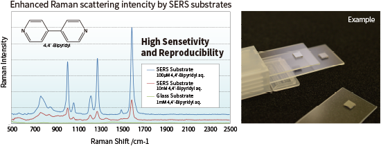
Application of Nano Dot Array 6, High sensitive SERS* substrates for Raman Spectroscopy

When light enters metal nanostructured surfaces, electromagnetic filed is amplified by surface plasmon resonance. In this field, Raman intensity of analyte is significantly enhanced (Surface Enhanced Raman Scattering), and it is used for high sensitive Raman spectroscopy analysis.

*SERS (Surface Enhanced Raman Scattering)
The figure shows the fields of use of SERS substrates. The center of the figure reads “Areas of Use of SERS Substrates,” and six applications are listed around it. They include general analytical applications, security fields, healthcare medical testing, pharmaceutical testing, food testing, and environmental testing, with specific analytical content (e.g., pathogen analysis, drug detection, pesticide residue, etc.) indicated for each application.

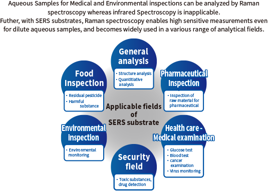
Characteristics of our SERS substrates.

SERS substrates with Au and Ag fine structures are available. Encouraged excitation wavelengths are 780nm for Au-SERS and 532nm for Ag-SERS substrates. For both types of SERS substrates, expiry date is about 3 months after shipment.

Graph and sample images showing Raman scattering intensity of SERS substrates. The graph shows Raman shift/cm-1 data, indicating that the SERS substrate exhibits higher Raman scattering intensity than the glass substrate. On the right, a sample example of a SERS substrate is shown, with a small square SERS substrate on a transparent substrate.
Application
Micro analysis such as environmental and pharmacentical inspection, Raw materials analysis, etc.
Specifically suitable for aqueous samples.
Materials
Au or Ag fine structures on silicon or glass substrates.